37+ Mos Fet Circuit Diagram PNG. The universal voltage divider biasing circuit is a popular biasing technique used to establish a desired dc operating condition of bipolar transistor amplifiers as well as mosfet amplifiers. This circuit shows that dimmers not only for to control mains voltage they can also control dc as well ac.
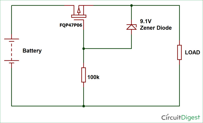
Reverse Polarity Protection Circuit using Diode OR P ... from circuitdigest.com Mosfet which has become the most commonly used three terminal devices brings revolution in the world of electronic circuits. As shown in the given circuit diagram the mosfet forms the main controlling device with practically no complications around it. A switch at its gate which can as shown in the diagram below, a capacitor is added just after the switch and across the 1m resistor.
Mosfet is a 3 terminal semiconductor device used in a wide range of electronic circuits.
In continuation of the previous discussion of si transistor types, features and basic characteristics, we here provide an additional explanation of the characteristics of si mosfets that are at present widely used as power switches. A power transistor (mosfet or igbt) is connected in parallel with a power diode with the polarities shown. A switch at its gate which can as shown in the diagram below, a capacitor is added just after the switch and across the 1m resistor. Start date oct 23, 2017.

0 Response to "Mos Fet Circuit Diagram"
Post a Comment